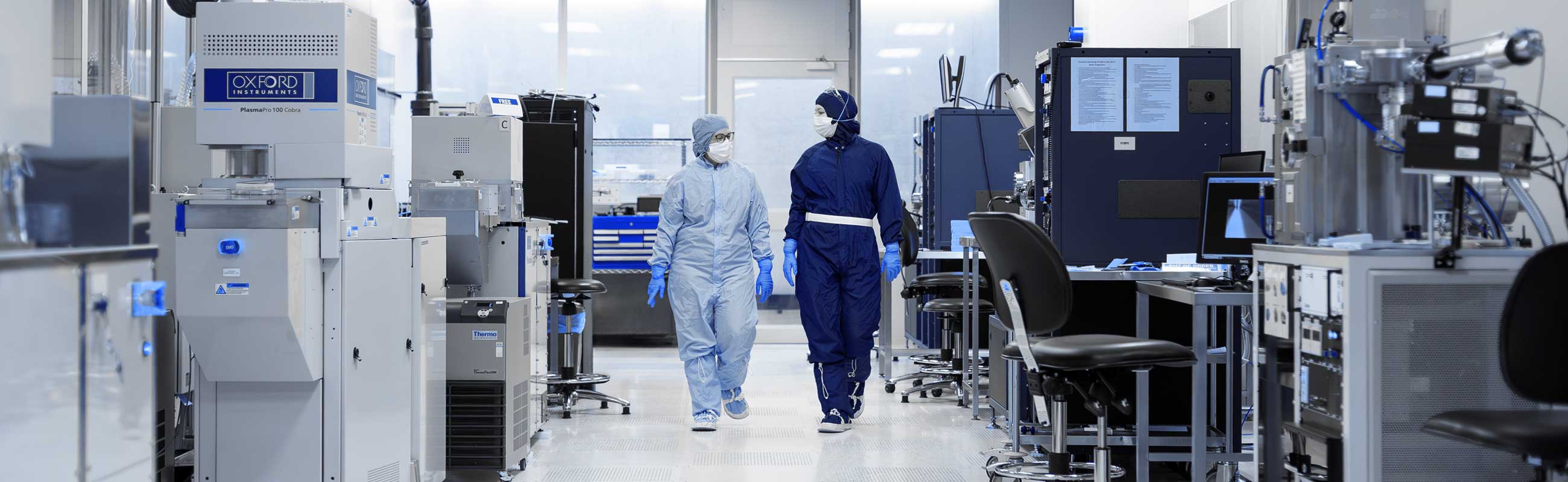
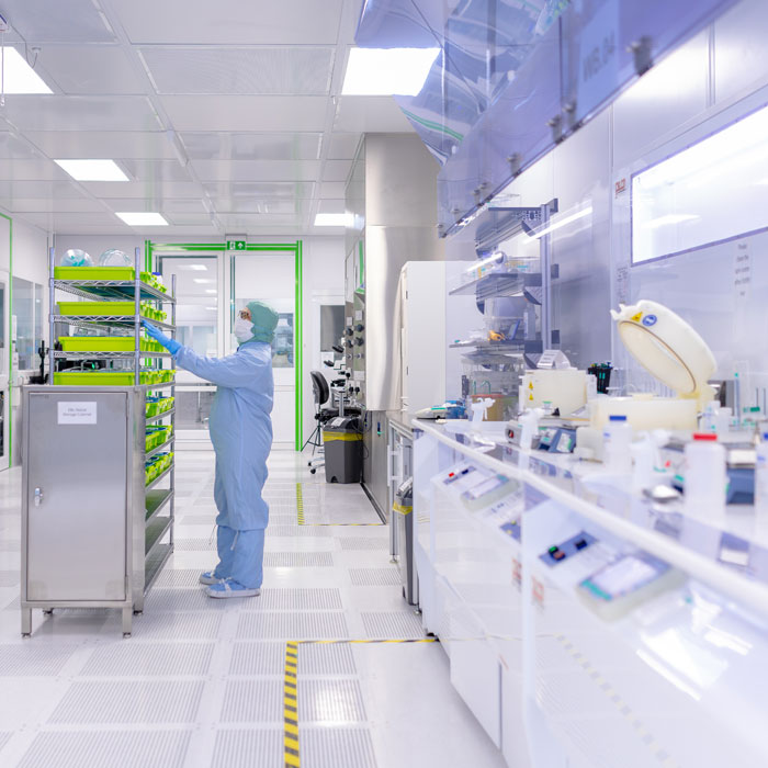
World-leading cleanroom facilities for 2D materials research
Our 1,500m² ISO class 5 and 6 cleanrooms house an unrivalled range of micro and nanofabrication equipment, purpose built to support every stage of 2D materials research and device development.
2D material preparation and handling
The 2D material handling and transfer facilities offer tools for isolating and transferring 2D materials under clean, controlled environments.
Capabilities include:
- General exfoliation
- Flake transfer rigs
- Inert atmosphere gloveboxes
- Ultra-high vacuum systems, ideal for sensitive material processing.
These resources support both academic research and industrial research and development in nanomaterials, enabling precise, contamination-free workflows.
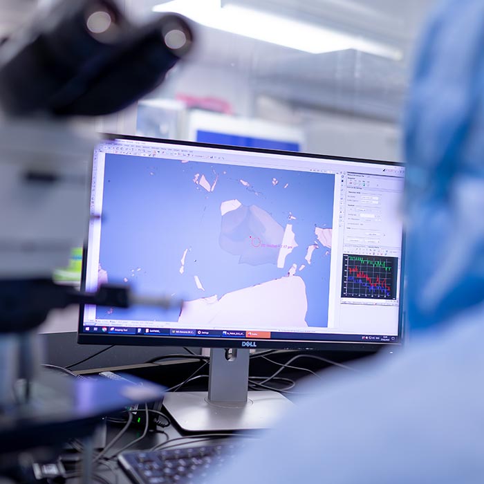
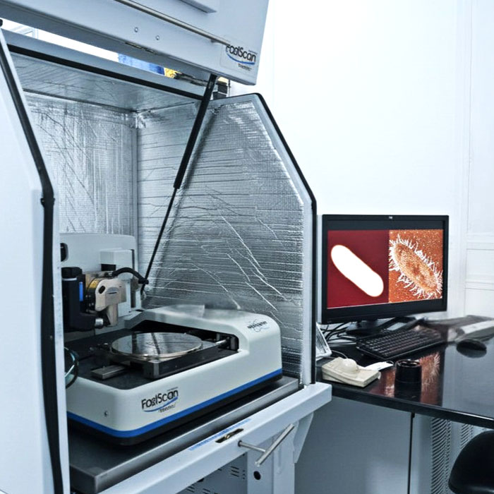
Characterisation
The characterisation tools offer a comprehensive suite for analysing 2D materials and nanostructures.
Tools include:
- Optical microscopy
- Scanning electron microscopy (SEM)
- Atomic force microscopy (AFM)
- Raman spectroscopy
- X-ray diffraction
- Imaging spectroscopic ellipsometry.
These tools enable detailed imaging, surface profiling, and material identification. Designed for both research and industrial applications, providing critical insight into material properties at the nanoscale, supporting quality control, device fabrication and fundamental studies.
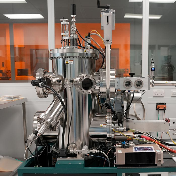
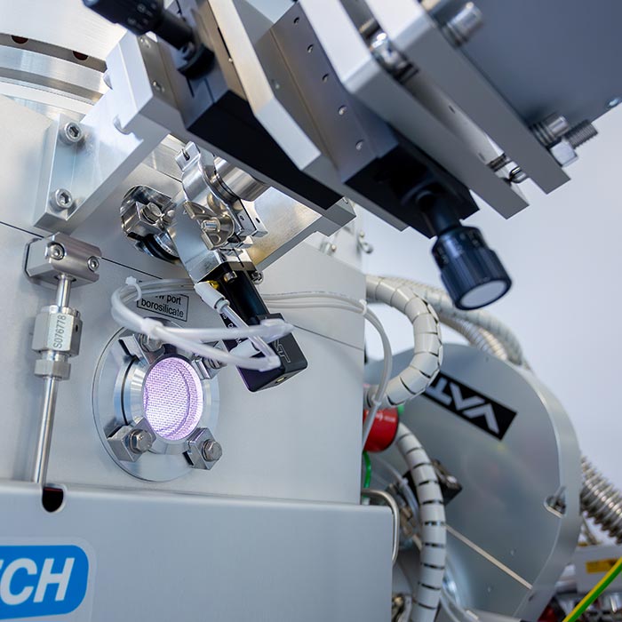
Deposition
The deposition equipment includes high-spec systems for thin-film growth and material coating, supporting precision engineering of 2D and nanomaterials.
Key technologies include:
- Plasma enhanced chemical vapour deposition (PECVD)
- Atomic layer deposition (ALD)
- Electron-beam and thermal evaporation
- Magnetron sputtering.
These tools enable tailored layer-by-layer construction and advanced heterostructure fabrication, essential for next-generation electronics, optoelectronics, and sensing platforms.
Electron-beam lithography (EBL) and focused-ion-beam (FIB)
This facility features high-performance systems for advanced nanoscale patterning and imaging. The setup includes:
- A range of scanning electron microscope (SEM)-based nanolithography systems
- A dedicated imaging SEM with energy dispersive X-ray spectrometry (EDS)
- A 100 kV dedicated EBL system for high-resolution large-area patterning
- A gallium focused ion beam system (FIB-SEM) for precise, site-specific milling, nanofabrication and sample preparation and analysis.

Wet chemistry
This area provides a dedicated space for chemical processing, offering a suite of surface treatment and cleaning protocols.
Capabilities include:
- Automated wet benches for reproducible sample preparation with RCA standard cleans 1 and 2
- Acid Piranha etch, Hydrofluoric (HF) acid etching in both liquid and vapour forms
- A variety of metal etchants, and KOH silicon etchant
These advanced processes ensure meticulous etching and cleaning essential for high-performance device fabrication.
Plasma etching
The suite provides advanced platforms for precise material removal and pattern transfer.
Capabilities include:
- High-performance reactive ion etching (RIE) systems
- Deep reactive ion etching (DRIE) capabilities
- Specialised tools for plasma and ion milling processes
These facilities enable fine-tuned etching of a range of materials, ensuring high resolution and selectivity critical for device fabrication.
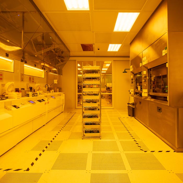
Photolithography
The Photolithography suite features advanced systems for high-resolution patterning and wafer processing.
Key equipment includes:
- Laser lithography
- UV and deep-UV mask aligners for precise transfer of micro- and nanoscale patterns.
Work in our cleanrooms
Find out how you can leverage all our unique facilities to benefit your research and development goals.
